Let’s Begin the Journey
Here in Prague, the design center focuses on current sensors, primarily using the Hall effect (mostly) or tunnel magneto-resistance (less commonly). The most important applications of these physical effects are:
- Hall switch: Used to detect when a current or magnetic field is applied in a particular direction.
- Magnetic latches: When the magnetic field is on the south pole, it is ON; when it is on the north pole, it is OFF.
- Linear devices: These provide an output voltage proportional to the input current/magnetic field, usually differential at half-supply of common mode.
The image below shows an example of a Hall switch.

Hall-based Current Sensors
Starting from theory, if we have electrons traveling through a material with velocity $\vec{v}$ in which a magnetic field $\vec{B}$ is applied, the Lorentz force will cause the electron to deviate from its original trajectory:
$$ \vec{F} = q \vec{v} \times \vec{B} $$
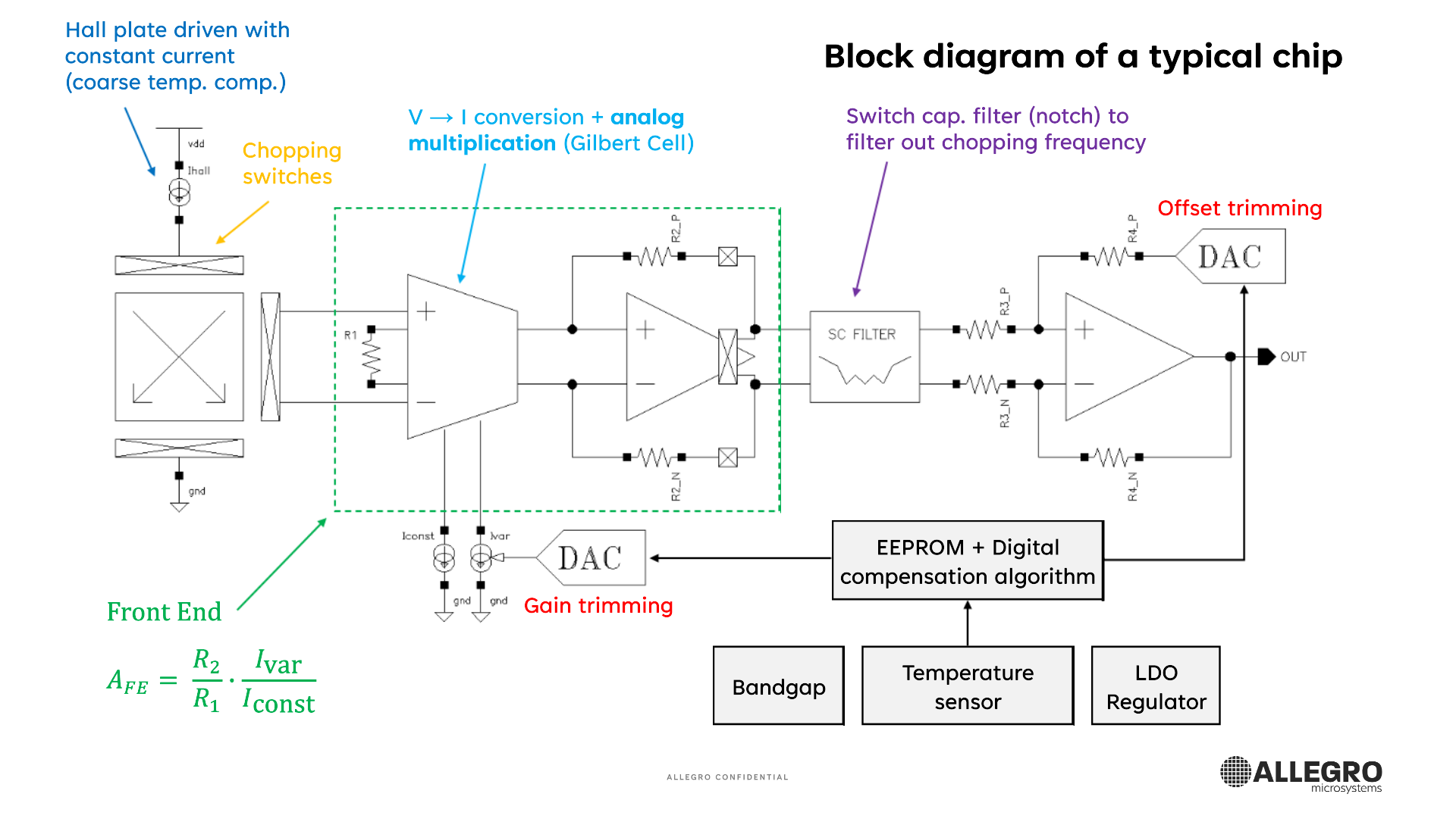
In Allegro’s design, a bias current is pushed inside a square silicon plate integrated into the chip, from one corner to another. If a magnetic field is present (due to currents near the Hall plate), the electron flow deviates towards the other two corners, creating a net charge. This charge is measured by an analog frontend.
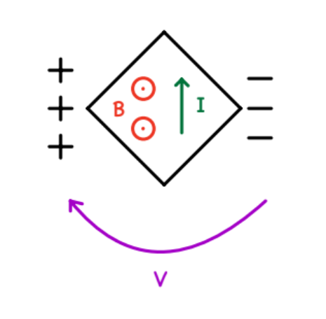 $V_{H} = \frac{I \ B_{\bot}}{p_{n} \ q \ t}$
Here, $V_{H}$ is the voltage created by the charge movement on the two corners orthogonal to the current flow. $p_{n}$ is the carrier density, $q$ is the charge, and $t$ is the thickness of the plate.
It’s clear that if the magnetic field changes direction, $V_{H}$ will reverse polarity.
Advantages of This Type of Current Sensing
- You don’t have to touch the wire to measure the current, so there’s no need for a shunt resistor, and the isolation between the sensor and the circuit in which the current flows is excellent.
- Imagine a fast current pulse creating a fast magnetic field pulse. These sensors are inherently fast and can follow that pulse. The maximum measurable frequency of a current signal is determined by the electronics.
- The Hall plate and electronics are typically integrated on a single chip.
Challenges to Overcome
-
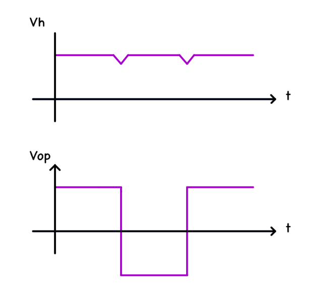
When no magnetic field is present around the plate (which is unlikely on Earth), you would expect $V_{H} = 0$. However, this is not the case. The voltage at which the output stands in zero current/field conditions is called the offset of the plate, $V_{op}$.
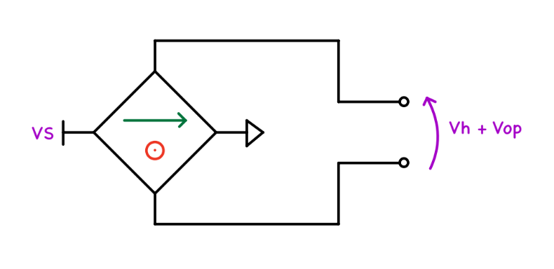
This is more of a statistical effect, varying from chip to chip, mainly due to geometrical asymmetries, the piezoresistive effect, resistance gradients along the plate, external fixed magnetic fields…etc. It’s not negligible (it can range from 0.5 to 5mV for a 5V power supply).
-
Signal-to-noise ratio: If you didn’t notice, the signal-to-noise ratio is an important issue.
$$ V_{H} = S_{v} \cdot B_{\bot} \cdot V_{s} $$
(where $S_{v} = 0.04 - 0.08 T^{-4}$, sensitivity per unit voltage)
The signal from the sensor is very small, typically in the tens of microvolts. Can you imagine electronics that don’t add tens of microvolts to the signal and degrade the noise figure? This poses serious issues for the electronic frontend. It’s not enough to simply increase the gain along the signal path, because the overall noise will also be amplified.
-
The Hall plate integrated into the chip behaves like a resistor (since it’s a piece of doped silicon through which current flows), so noise is generated from it. Additionally, there is a huge drift in its value due to temperature changes and aging. A large part of the work inside the chip focuses on correcting for temperature drift.
How Allegro Tackles These Issues
-
Offset ➡️ The voltage coming from the plate is chopped, shifting the offset voltage to high frequencies, which are then filtered. In the image below, the magnetic field $\vec{B}$ is considered constant, and $V_{H}$ is a DC signal.
-
S/N ➡️ Allegro uses a BCD technology in which the first stage is bipolar, keeping offset and noise low. This achieves a good compromise between gain and noise degradation. The plate resistance should be minimized, but there are technological limits, so multiple plates are used in parallel (more area ❗). The noise from the plate can also be mitigated by increasing the bias current (which increases power consumption ❗).
-
Temperature and aging ➡️ The electronics form a “giant” feedback loop, where the analog frontend amplifies and filters the signal from the plate. This information is then used to calibrate the analog part via embedded digital circuitry, based on complex model-based design. This allows the analog frontend to adapt to changing environmental and lifetime conditions.
What’s Next?
In the next episode, I will summarize the circuit design techniques behind the three points mentioned above. Then, I will describe my role in this company.